﹤Semiconductor Technologies﹥Development of single-crystal technology for two-dimensional semiconductor materials
National Sun Yat-sen University / Prof. Chang-Hsiao Chen
Pain Points Solved
The advanced semiconductor industry is hailed as a pillar of the nation, with TSMC further expanding its investments in the US and Japan. Meanwhile, Moore's Law is facing bottlenecks, prompting scientists worldwide to consider next-generation semiconductor materials and devices. Two-dimensional (2D) materials are among the key channel materials known to be able to solve technology nodes below 1 nm, and are a field that advanced semiconductor industries both domestically and internationally are vying to develop. Bilayer 2D devices have proven to have significantly superior performance compared to monolayers. However, limited growth thermodynamics and the lack of dangling bonds make it difficult to synthesize highly uniform bilayers. To date, all reports on fully monocrystalline 2D materials have used monolayer architectures. Developing both bilayer and fully monocrystalline 2D material growth technologies is crucial for future electronic applications.
Technology Introduction
We employed a two-step method to directly grow bilayer all-single-crystal MoS2. AFM observation revealed the morphology of the bilayer MoS2 sample. The second layer exhibited a layered morphology and uniaxial, co-directional growth, with a horizontal crystal size of approximately 8–10 μm, a height difference of 0.7 nm from the first layer (Figure 1a). OM observation showed that the second layer also grew in a triangular morphology, aligned with the first layer, exhibiting 3R-type stacking (AA stacking) (Figure 1b). Raman and PL spectral analysis confirmed its bilayer MoS2 characterization (Figure 1c). In terms of electrical performance verification, under the stringent condition of a long-channel gate length of 25 μm, the average mobilities of the bilayer and single-layer MoS2 transistors were 48 and 9 cm²V⁻¹s⁻¹, respectively, representing a significant increase of more than five times. Simultaneously, excellent current on/off ratios of 10⁸ and 10⁷ were achieved, respectively (Figure 1d). More importantly, we noticed that our second layer of MoS2 is formed by stacking 3R single layers to create a double-layer all-monocrystalline MoS2, which is different from the mixed 2H and 3R twins used by China teams.

Figure 1. Synthesis of bilayer monocrystalline MoS2: (a) AFM shows the layered morphology of the bilayer; (b) OM analysis shows the co-directional alignment and 3R stacking of the bilayer; (c) Raman and PL verification of the number of layers; (d) Electrical analysis of bilayer and monolayer monocrystalline MoS2 devices.
Application Examples
Development of Next-Generation Advanced Semiconductor Materials and Devices
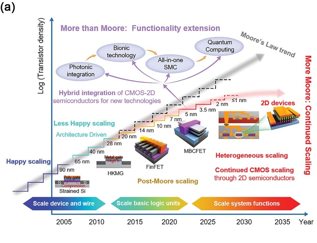
Figure 2. Evolution of transistor architectures and materials across generations. Two-dimensional semiconductor materials are expected to be introduced into semiconductor manufacturing processes by 2030.
Related Links
Patent Name and Number
None
Industry-Academia / Tech Transfer Partner
None
Honors and Awards
None
Technical Contact
Industrial Liaison Office
National Sun Yat-sen University
Tel: +886 7-5250165
Email: gloria@mail.nsysu.edu.tw